- 您现在的位置:买卖IC网 > Sheet目录2000 > ISD5008EYI (Nuvoton Technology Corporation of America)IC VOICE REC/PLAY 4-8MIN 28-TSOP
ISD5008
Publication Release Date: Oct 31 2008
- 22 -
Revision 1.2
6.4.4
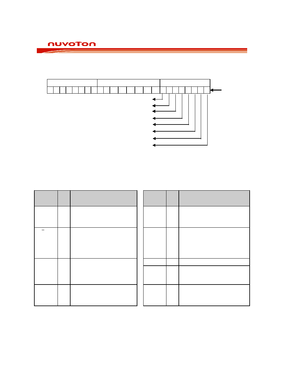
SPI Port
The following diagram describes the SPI port and the control bits associated with it.
Byte 1
Byte 2
Byte 3
D0 D1 D2 D3 D4 D5 D6 D7 D8 D9 D10 D11 D12 D13 D14 D15 C0 C1 C2 C3 C4 C5 C6 C7
MOSI
Reserved
Load CFG0 (LC0)
Load CFG1 (LC1)
Message Cueing
Ignore Address Bit
PowerUp
Play/Record
Run
6.4.5
SPI Control Register
The SPI control register provides control of individual device functions such as Play, Record, Message
Cueing, Power-Up and Power-Down, Start and Stop operations, Ignore Address Pointers and Load
Configuration Registers.
TABLE 7: SPI CONTROL REGISTER
Control
Register
Bit
Device Function
Control
Register
Bit
Device Function
RUN
=
1
0
Enable or Disable an operation
Start
Stop
PU
=
1
0
Master power control
Power-Up
Power-Down
P/
R
=
1
0
Selects Play or Record operation
Play
Record
IAB
=
1
0
Ignore address control bit
Ignore input address register (A15-
A0)
Use the input address register
contents for an operation (A15-A0)
MC
=
1
0
Enable or Disable Message
Cueing
Enable Message Cueing
Disable Message Cueing
A15-A0
Output of the row pointer register
D15-D0
Input control and address register
LC0
=
1
0
Load Configuration Reg 0
No Load
LC1
=
1
0
Load Configuration Reg 1
No Load
发布紧急采购,3分钟左右您将得到回复。
相关PDF资料
ISL12008IB8Z
IC RTC I2C LO-POWER 8-SOIC
ISL12020MIRZ-T7A
IC RTC/CALENDAR TEMP SNSR 20DFN
ISL12022IBZ-T7A
IC RTC/CALENDAR TEMP SNSR 8SOIC
ISL12022MAIBZ
IC RTC/CALENDAR TEMP SNSR 20SOIC
ISL12022MIBZ-T7A
IC RTC/CALENDAR TEMP SNSR 20SOIC
ISL12022MIBZR5421
IC RTC/CALENDAR TEMP SNSR 20SOIC
ISL12023IVZ
IC RTC/CLDR TEMP SNSR 14-TSSOP
ISL12024IRTCZ
IC RTC/CALENDER 64BIT 8-TDFN
相关代理商/技术参数
ISD5008P
功能描述:IC VOICE REC/PLAY 4-8MIN 28-DIP RoHS:否 类别:集成电路 (IC) >> 接口 - 语音录制和重放 系列:ISD5008 标准包装:14 系列:- 接口:串行 滤波器通频带:1.7kHz 持续时间:8 ~ 32 秒 安装类型:通孔 封装/外壳:28-DIP(0.300",7.62mm) 供应商设备封装:28-PDIP 其它名称:90-21300+000
ISD5008PY
功能描述:IC VOICE REC/PLAY 4-8MIN 28-DIP RoHS:是 类别:集成电路 (IC) >> 接口 - 语音录制和重放 系列:ISD5008 标准包装:14 系列:- 接口:串行 滤波器通频带:1.7kHz 持续时间:8 ~ 32 秒 安装类型:通孔 封装/外壳:28-DIP(0.300",7.62mm) 供应商设备封装:28-PDIP 其它名称:90-21300+000
ISD5008S
功能描述:IC VOICE REC/PLAY 4-8MIN 28-SOIC RoHS:否 类别:集成电路 (IC) >> 接口 - 语音录制和重放 系列:ISD5008 标准包装:14 系列:- 接口:串行 滤波器通频带:1.7kHz 持续时间:8 ~ 32 秒 安装类型:通孔 封装/外壳:28-DIP(0.300",7.62mm) 供应商设备封装:28-PDIP 其它名称:90-21300+000
ISD5008SD
制造商:未知厂家 制造商全称:未知厂家 功能描述:SINGLE CHIP VOICE RECORD PLAYBACK DEVICE 4-, 5-, 6-, AND 8- MINUTE DURATIONS
ISD5008SERIES
制造商:未知厂家 制造商全称:未知厂家 功能描述:Single-Chip Voice Record/Playback Device
ISD5008SI
功能描述:IC VOICE REC/PL 4-8MIN IN 28SOIC RoHS:否 类别:集成电路 (IC) >> 接口 - 语音录制和重放 系列:ISD5008 标准包装:14 系列:- 接口:串行 滤波器通频带:1.7kHz 持续时间:8 ~ 32 秒 安装类型:通孔 封装/外壳:28-DIP(0.300",7.62mm) 供应商设备封装:28-PDIP 其它名称:90-21300+000
ISD5008SIR
功能描述:IC VOICE REC/PL 4-8MIN IN 28SOIC RoHS:否 类别:集成电路 (IC) >> 接口 - 语音录制和重放 系列:ISD5008 标准包装:14 系列:- 接口:串行 滤波器通频带:1.7kHz 持续时间:8 ~ 32 秒 安装类型:通孔 封装/外壳:28-DIP(0.300",7.62mm) 供应商设备封装:28-PDIP 其它名称:90-21300+000
ISD5008SY
功能描述:IC VOICE REC/PLAY 4-8MIN 28-SOIC RoHS:是 类别:集成电路 (IC) >> 接口 - 语音录制和重放 系列:ISD5008 标准包装:14 系列:- 接口:串行 滤波器通频带:1.7kHz 持续时间:8 ~ 32 秒 安装类型:通孔 封装/外壳:28-DIP(0.300",7.62mm) 供应商设备封装:28-PDIP 其它名称:90-21300+000